In today’s fast-moving electronics industry, SMT PCB Assembly (Surface Mount Technology Printed Circuit Board Assembly) has become the backbone of modern device manufacturing. From smartphones and wearables to automotive systems and medical devices, SMT offers the speed, precision, and miniaturization required for next-generation products.
This complete guide explains how SMT PCB Assembly works, why it’s essential, and how manufacturers can optimize it for efficiency, performance, and cost savings.
What Is SMT PCB Assembly?
SMT PCB Assembly is a manufacturing process where electronic components are mounted directly onto the surface of a printed circuit board (PCB), instead of inserting leads through holes. This enables:
- Smaller, more compact device designs
- Higher density of components
- Faster and automated production
- Improved electrical performance
According to IPC — a global electronics standards organization — more than 90% of today’s PCB assemblies use SMT due to its speed and precision.
Why SMT PCB Assembly Dominates Modern Electronics Manufacturing
SMT isn’t just a trend — it’s a fundamental technology enabling modern electronics. Here’s why:
1. Miniaturization for High-Tech Devices
SMT allows extremely small components like:
- Resistors
- Capacitors
- ICs
- BGA packages
- Microcontrollers
This enables ultra-thin laptops, smartwatches, IoT sensors, and more.
2. Automation and High Speed
Automated pick-and-place machines can mount tens of thousands of components per hour, drastically reducing labor costs.
3. Reliability and Performance
SMT components provide:
- Lower parasitic inductance
- Better high-frequency performance
- Improved thermal stability
4. Cost Efficiency
SMT reduces:
- Board size
- Manufacturing steps
- Material waste
- Overall per-unit cost
How the SMT PCB Assembly Process Works (Step-by-Step)
Below is a complete breakdown of each stage in the SMT process.
1. Solder Paste Printing
A stencil printer applies solder paste onto PCB pads.
Goals:
- Exact amount of paste
- Clean, accurate pad coverage
- Strong solder joints
Poor printing causes up to 60% of SMT defects, according to research by Electronics Weekly.
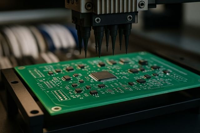
2. Pick-and-Place Component Mounting
High-speed robots pick components from reels/trays and place them precisely onto the solder-pasted PCB.
Common SMT components include:
- 0402 & 0603 resistors
- QFN chips
- BGA processors
- SOT/SOP packages
Pick-and-place accuracy often reaches ±0.01 mm.
3. Reflow Soldering
The PCB enters a reflow oven where solder paste melts and permanently bonds components.
Reflow stages:
- Preheat
- Soak
- Reflow (peak temperature)
- Cooling
Lead-free solder typically peaks around 240–245°C.
4. Automated Optical Inspection (AOI)
Cameras inspect:
- Component alignment
- Solder joints
- Missing/shifted parts
- Tombstoning
- Shorts/bridges
Modern AOI systems use AI for improved defect detection.
5. X-Ray Inspection (for BGAs/QFNs)
Essential for hidden-lead components.
Detects:
- Voids
- Head-in-pillow defects
- Open joints
6. Functional Testing
This verifies that the assembled PCB works as intended.
Methods:
- ICT (In-Circuit Testing)
- FCT (Functional Circuit Test)
- Boundary scan
- Environmental testing
SMT PCB Assembly vs. Through-Hole Assembly (Comparison Table)
| Feature | SMT PCB Assembly | Through-Hole Assembly |
|---|---|---|
| Component Size | Very small | Larger |
| Mounting | Surface-mounted | Hole-inserted |
| Automation | Highly automated | Semi-automated/manual |
| Strength | Ideal for high frequency | Better for mechanical stress |
| Cost | Lower | Higher |
| Speed | Very fast | Slower |
| Applications | Consumer electronics, IoT, medical | Power devices, connectors, aerospace |
Types of SMT Components Used in PCB Assembly
1. Passive Components
- Capacitors
- Resistors
- Inductors
2. Active Components
- Transistors
- Diodes
- Integrated circuits
3. IC Packages
- BGA
- QFN
- SOIC
- TSOP
- CSP
4. Specialized Components
- RF modules
- MEMS sensors
- LEDs
These components allow manufacturers to create feature-rich compact designs.
Equipment Used in SMT PCB Assembly
Modern SMT lines use a variety of advanced machines:
1. Solder Paste Printer
Applies paste onto pads using stainless steel stencils.
2. Pick-and-Place Machine
High-speed robotic arms assemble components.
3. Reflow Oven
Melts solder paste using multi-zone heating.
4. AOI Machines
Automated optical inspection for quality control.
5. X-Ray Inspection System
For hidden-lead components like BGAs.
6. Rework Stations
Used to fix soldering defects or replace faulty components.
Advantages of SMT PCB Assembly
SMT brings several engineering and cost benefits:
1. Higher Component Density
More components per square inch.
2. Improved Performance
Better RF and high-frequency characteristics.
3. Lower Production Costs
Automation reduces labor and time.
4. Smaller, Lighter Products
Ideal for wearable and portable devices.
5. Faster Manufacturing
Machines can place thousands of components per minute.
Challenges and Solutions in SMT PCB Assembly
Challenge 1: Tombstoning
Cause: Uneven heating.
Solution: Optimize reflow profile.
Challenge 2: Solder Bridges
Cause: Excess solder.
Solution: Better stencil design.
Challenge 3: Misalignment
Cause: Vibrations or wrong pick-and-place settings.
Solution: Calibrate equipment regularly.
Challenge 4: Voids in Solder Joints
Cause: Moisture or wrong profile.
Solution: Pre-bake components.
Case Study: SMT PCB Assembly in IoT Device Manufacturing
A leading IoT manufacturer upgraded from manual assembly to fully automated SMT PCB Assembly.
Results after 6 months:
- Production speed increased by 320%
- Defect rate dropped by 70%
- Unit cost reduced by 28%
- Product reliability improved significantly
This demonstrates how SMT can scale IoT manufacturing rapidly and cost-effectively.
Cost Factors in SMT PCB Assembly
Several elements influence assembly pricing:
1. PCB Design
- Layer count
- Complexity
- Trace width
- Via type
2. Component Types
- BGA and QFN packages cost more
- Rare or custom parts increase cost
3. Order Volume
Higher volume = lower per-unit cost.
4. Testing Requirements
Advanced tests add to total cost.
5. Assembly Difficulty
Fine-pitch components increase labor and machine time.
Best Practices for High-Quality SMT PCB Assembly
Follow these tips to ensure optimal results:
1. Follow IPC Standards
Standards like IPC-A-610 ensure quality and reliability.
2. Use Proper Thermal Profiling
Correct reflow profiles reduce defects dramatically.
3. Optimize Design for Manufacturability (DFM)
- Correct pad sizes
- Sufficient spacing
- Defined solder masks
4. Regular Machine Maintenance
Reduces placement and soldering errors.
5. Keep Components Moisture-Free
Store in dry cabinets to prevent failure.
FAQs
1. What is SMT PCB Assembly?
SMT PCB Assembly is the process of mounting electronic components directly onto the surface of a PCB using solder paste, pick-and-place machines, and reflow soldering.
2. Why is SMT better than through-hole?
SMT offers smaller components, higher speed, lower cost, and better performance for modern electronic devices.
3. What equipment is needed for SMT PCB Assembly?
Key equipment includes a solder paste printer, pick-and-place machine, reflow oven, AOI, and X-ray inspection system.
4. What causes defects in SMT Assembly?
Common causes include improper solder paste application, incorrect reflow profiles, and component misalignment.
5. Can SMT be used for all electronics?
Most devices use SMT, but through-hole is still used for connectors, heavy components, and high-stress applications.
Conclusion: Why SMT PCB Assembly Is Essential for Modern Manufacturing
In an era where electronic devices are becoming smaller, faster, and more powerful, SMT PCB Assembly stands out as the most efficient and reliable method for manufacturing high-quality PCBs. Its combination of automation, precision, cost efficiency, and scalability makes it indispensable for industries like consumer electronics, telecommunications, automotive, aerospace, and IoT.
By mastering best practices, using advanced equipment, and following IPC standards, manufacturers can significantly enhance performance, reduce defects, and create cutting-edge products that meet global market demands.